Clamping circuits have the advantage of not fully disconnecting the load during the OV event, instead dissipating some of the unwanted energy across a pass element such as a MOSFET.
Passive: Zener Diode Clamp
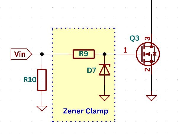
Pros of this circuit:
- Simple with few parts
- Effective at clamping voltage sources that do not supply a high amount of current (used in protecting MOSFET gates which are high-impedance).
Cons:
- Limited accuracy based on the reverse conduction curve of the Zener diode. Although, there are parts such as the TL431 shunt regulator which can replace Zener diodes with higher accuracy.
- Clamping capability is limited by the dynamic impedance and power dissipation of the Zener diode.
Active: Transistor-based Clamp
A linear voltage regulator is a transistor-based voltage clamp:
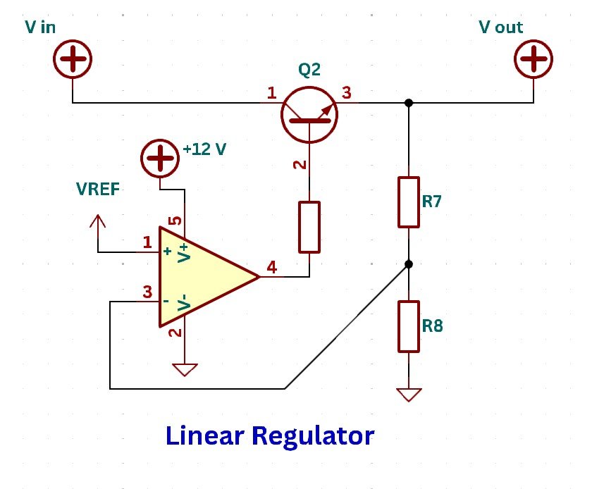
The op-amp drives the transistor (Q2) in its linear region to drop the required voltage such that the voltage at the non-inverting terminal matches the reference voltage.
Pros of this circuit:
- Useful for situations where frequent, small amounts of over-voltage are present and forcing a hard-disconnect isn’t desirable.
- Does not disconnect the load so your device remains functioning as normal as long as the voltage is able to be clamped.
Cons:
- Can easily fail if the energy dissipated becomes too high, thus it is wise to add temperature monitoring of the pass element. For this reason alone, we do not like to work with active clamp circuits unless the FETs are packaged in an IC with temperature monitoring.
- Transistor pass element fails short if over-stressed, so it is not intrinsically safe.
- When in non-clamping mode, the transistor still adds a small amount of series resistance to the power path, raising questions about voltage drop and heat dissipation.
Switched disconnect circuits do not require temperature monitoring and are suitable for a wide array of applications. There are two general types on the market; those using relays and others using semiconductors. The biggest differences between the two are isolation voltage and response time, which we will discuss here.
Switched P-MOSFET:
Shown below is an OVP circuit based on a rail-rail comparator driving a P-channel MOSFET [1].
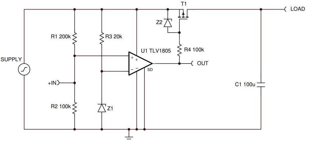
When 1/3 of +IN is higher than the reference voltage given by Z1, the comparator is high and the MOSFET gate-source voltage is approximately 0, meaning the transistor shuts off. R4 limits the current to the gate of the MOSFET when the comparator is driving it high and limits the flow of current through Z2 when the comparator is low.
Pros of this circuit:
- Simple to design with few parts. Just find a good, low-resistance P channel MOSFET that has a high enough drain-source voltage for your application.
- Extremely fast response when compared to a crowbar or relay-based circuit (10’s of microseconds response time possible).
- Easy to add soft-start for OVP on start-up by adding RC network to MOSFET gate, at the expense of inrush-current performance.
- Identical or similar parts can be used to make a window comparator for both under-voltage and over-voltage.
Cons:
- Vulnerable to noise on input supply. Without an additional hysteresis resistor between OUT and the inverting input, the comparator will rapidly switch when 1/3 of +IN is at the Zener reference voltage. This can cause rapid heating and potential destruction of the MOSFET.
- High series voltage drop and limited efficiency due to the use of a P-channel MOSFET, especially at lower input voltages where the Vgs is not >> threshold.
- Not widely adjustable over a large voltage range.
- Limited accuracy due to change of Zener breakdown voltage with temperature and current. Using a TL431 Zener shunt regulator for greater accuracy is recommended.
- Only rated as high as the MOSFET (and comparator), and fails short if exposed to extreme over-voltages (not intrinsically safe).
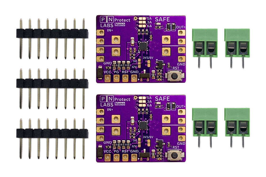
PN Labs Protect module:
The Protect module is an improvement to many of the shortcomings of the circuit shown above. It is a switched-MOSFET circuit that has exceptional efficiency, and a wide-adjustable range from 5-30 V up to 25 A. It is rated to protect up to 40 V DC.
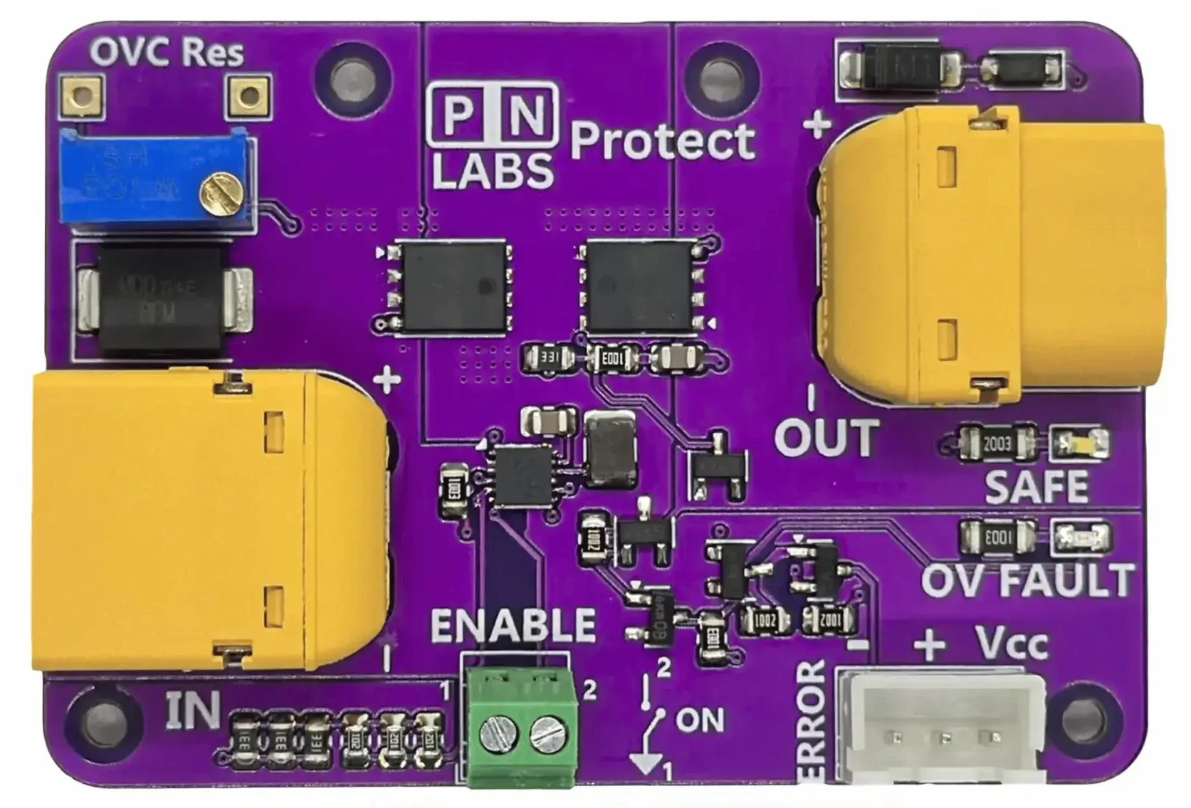
Pros of this circuit:
- Ultra-fast response time in tens of μs or faster.
- True over-voltage protection, with soft-start, for protecting immediately on power-up. It also has additional features, such as reverse polarity and reverse current blocking due to the use of a back-back FET architecture.
- Exceptional efficiency due to use of high-performance N-channel MOSFETs (over 99% typical)
- Enable switch terminal for direct ON/OFF control.
Cons:
- Only rated up to 40 V DC of blocking, limited by the MOSFETs.
- More expensive than traditional relay circuits. High quality FETs, dedicated ASIC with built-in comparators and gate drivers are used.
- Soft-start limits the max allowable inrush current to 12.5 A upon start-up.
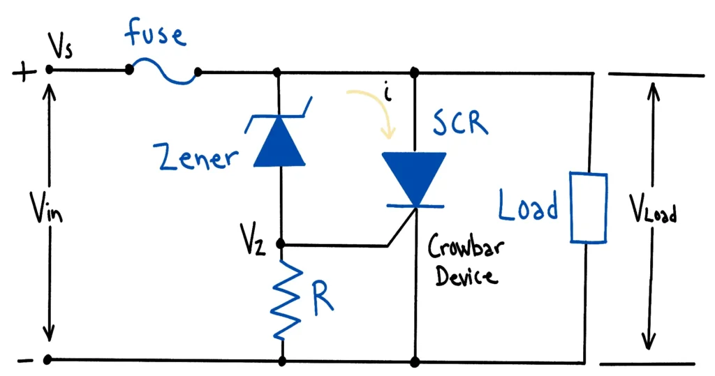
Switched Relay:
Most commercially available over and under voltage circuits are based on relays, for two reasons:
- Relay circuits built properly are almost guaranteed to fail open when they die, so they are intrinsically safer.
- Low-current relays are inexpensive and easy to design into a circuit.
A schematic of a typical relay-based OVP circuit with a comparator, relay, and n-channel MOSFET is shown below.
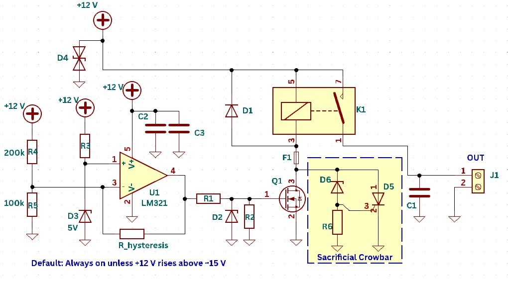
The comparator circuit turns on and off the MOSFET, which switches a relay in the main power path. The trip point is when 1/3 of the input voltage (nominally 12 V) goes above 5 V given by the Zener reference. A sacrificial crowbar circuit can be made to permanently shutoff the relay at the absolute max voltage of the circuit, at which point the high isolation voltage of the open relay will prevent high voltages from reaching the rest of the circuit.
Pros of this circuit:
- Cheap to build. No expensive MOSFET gate drivers required.
- Relays easily offer higher isolation voltage than a MOSFET would, and a sacrificial crowbar is built-in to force the relay open by blowing F1 in case of an extreme OV event
- Very low series voltage drop, since there is only K1’s switch in the power path.
Cons:
- Arc suppression inside the relay becomes more important as operating voltage and rated current increases. MOSFETs are inherently better at switching large amounts of current for this reason provided their SOA is respected.
- Short lifespan. Relay lifespans quoted in datasheets are often measured in “dry” conditions. In real life, the interruption of current will result in an arc being formed, which will damage the contacts slightly with each use. This eventually leads to the failure of the relay.
- Slow acting. Many relays have switching times of a few ms, which is several orders of magnitude longer than solid-state approaches.
Energy diversion circuits are deployed in systems where a hard-disconnection of the power supply could cause damage, such as hydroelectric generators or wind turbines. In these systems, the electrical load provides braking torque to slow down the rotor. If the load is suddenly disconnected, this braking is lost, potentially leading to a dangerous runaway condition. Instead of disconnecting the load, a pair of switches is activated to connect a “load-dump” resistor in parallel with the load, diverting excess energy and reducing the system voltage.
Here’s a load dump circuit created by Tim Williams from Seven Transistors Labs that is annotated for clarity [2]:
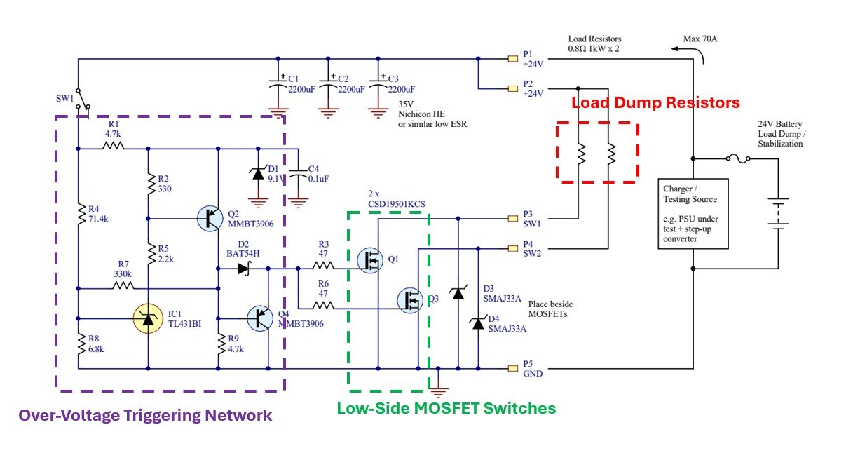
You can view his original post here. In this case, the gates of the two MOSFETs are tied together, which means that the two power resistors work together. Another approach could be to activate each resistor in two stages, corresponding to light and severe over-voltage events.
Pros of this circuit:
- Reliable way of protecting generators/flywheel systems where hard-disconnect is dangerous or impractical.
- Can be altered to dump increasing amounts of energy based on over-voltage level by triggering one/both resistors
Cons:
- Power resistors are generally bulky, and sized for the worst-case load conditions.
- Large amounts of heat generated
- Does not actually interrupt fault conditions, so damage is still possible if the load dump is ineffective.