


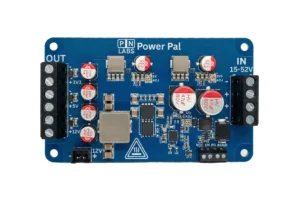
Description
- Selectable voltage output of 3.3, 5, 9 or 12 V using solder jumpers. Up to 36 V input voltage with 40 V absolute max.
- Current output of 2-2.5 A continuous, see maximum current vs input voltage plot.
- Over-current and thermal shutdown with auto retry. See datasheet for more details
- Enable and Power Good pins for remote operation and fault monitoring.
- 4 ms soft-start to help with smooth turn on and highly capacitive loads.
- SMT compatible with castellated edges make it suitable for soldering to a larger PCB as a module.
- Breadboard compatible with 2.54 mm flat or right angle header pins (included).
- High quality heatsink supplied with thermal tape to use for increasing the current output. Compare the levels of current attainable with and without it in the documentation.
By using the adjustable TPSM33625 step down voltage regulator IC with inductor-less switching technology, the NanoBuck boasts high efficiencies of 80-95% at continuous currents of up 2.5 A with the supplied heatsink. The actual current achievable depends on the ambient temperature, input voltage, and whether you use the heatsink. See the supplied graph for more details.
Why Integrated Inductor Technology is better:
Unlike conventional buck regulators that rely on bulky external inductors, integrated inductor technology embeds the inductor directly into the package alongside the controller and switching elements. This integration reduces PCB footprint, increases power density, and simplifies board layout by eliminating the critical high-current loop from the external design.
With the inductor shielded and internally packaged, parasitic resistance and inductance are minimized, enabling higher switching frequencies with lower losses and improved transient response. This results in better efficiency, reduced radiated EMI and an overall smaller footprint.
The IC also incorporates Dual Random Spread Spectrum (DRSS) technology to reduce EMI peaks.
Additional Resources
Learn more information to effectively use the NanoBuck in a variety of applications. All content belongs to the original owners, which we have linked.
[Soldering a PCB with Castellated Edges to a Larger PCB]:
- A really good tutorial and video by Sparkfun Electronics: (Website)
- Make sure to check out the Downloads tab for the recommended footprint
[Power Sequencing]:
- Why is Power Sequencing Needed? (Microchip Blog)
See it in action
IMSAI Guy’s NanoBuck product showcase – November 2025


Very good product, not many low cost voltage regulators have such good documentation.